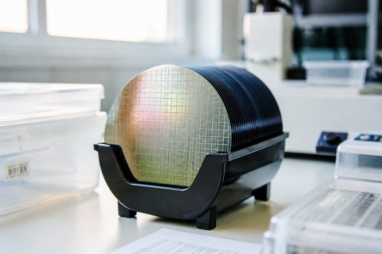
p
Applied Materials and Lam Research change the wafer. KLA reads it. Inspection is a wafer. Mix those two jobs and a process-control filing gets graded as a second deposition tool.
p
Semiconductors are fabricated on silicon wafers through deposition, patterning, material removal, heat treatment, and measurement and inspection. That last pair is not a courtesy. The 10-K for the year ended 30 June 2026 already put measurement and inspection on the same list as the film. Yield is a measured map.
h2
Inspection is a wafer
p
Inspection looks at the disc. Patterned wafers, unpatterned wafers, reticles. The object is the wafer in the boat, not a stamp at the end of the line. A foundry can name a node. It cannot yield that node without a map of what printed.
p
Metrology is the other half of the same object. Overlay, critical dimension, film thickness. Those are measurements, not options. A scanner that printed a window still has to land on the last layer. The EUV page already spent that window. This page is whether anyone measured it.
The map is the product. The film is someone else's catalog.